

PCB manufacturer brings a brief introduction to E-Test
Article source:Ribom Dated :04-21/2015
E-Test is used to detect the electrical performance of PCB. It is the essential process before shipment. New let PCB manufacturer explains the details of how to do E-Test on PCB.
1, Electrical function test:
The PCB defect caused by external factors during PCB process flow is unavoidable. The impact to cost is various and better to identify the defect as early as possible to reduce the loss. “The Rule of 10’s” aims to evaluate the remedy cost of the defect in different process. For example, if the trace open is found on the bare board, the failure location could be repaired or the bare board has to be scrapped. On the other hand, the cost will be increased when PCB goes to the next stage when it is assembled with components, mainly are the sorting cost, component cost and processing cost. The compensation ratio is 10 times or even more than the PCB cost and this damages PCB manufacturer’s profit. The worse case is when PCBA is installed onto the end product, the loss caused by defected PCB could be very painful, say up to thousand times of PCB cost. Therefore, the E-Test plays important role in PCB industry to segregate PCBs with defects from shipment to customers and that’s why most of customers require their PCB suppliers to do 100% E test before shipment.
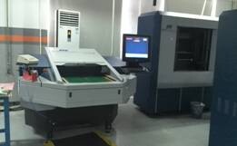
2, How to do e-test?
There are many methods for E-test, dedicated, universal grid, flying Probe, E-Beam, conductive fabric, capacity and ATG-SCAN MAN. The most popular 3 are: dedicated, universal grid and flying probe.
To get a better understanding to the features of this 3 types of E-test, let’s the comparison below:
1). The dedicated tester is specialized for a part number only; it can’t be applied to the others and recycled. And the testing points are around 10240 for single side PCB, 8129 for double side. The density is limited by the size of the probe size, it is applied the fine pitch PCB generally.
2). The universal grid tester is designed according to the circuit distribution of PCB. The grid distance is defined by the density of circuits and represented by the spacing. Only does the testing probe penetrates the solder mask to contact the holes, the fixture is easy to build and the probes can be recycled. There are many standard grid probe plates with all kinds of types for testing pads. It is convenient to build the active grid probe plate for different part numbers. During the mass production, different part number can be tested according to change the active grid probe plate. The universal grid tester is satisfied with the QFP PCB type.
3). Flying probe tests depends on the XYZ servo-system movement of 2 probes to test vias, component pads and circuit interconnects on both side of PCB at end point of electrical net. The testing speed is about 1000points/minute only because of the limitation by the end point net. That’s why the flying probe is suitable for the small volume/ prototype and the high density PCB.
Factory address: Mintai Industrial Park, Guantang Road, Huangjiang Town, Dongguan City, Guangdong Province
Office Address: Room 801, Dongtang Yongdongxing Building, Shajing Street, Bao'an District, Shenzhen
86-0755-33134847
86-0755-29868282


