

Dry Goods Sharing | Importance of PCBA Board Side Device Layout
Article source:PCBworld Dated :2023/01-10
The reasonable layout of electronic components on the PCB board is an extremely important step in reducing welding defects! Components should avoid areas with very large deflection values and high internal stress areas as much as possible, and the layout should be as symmetrical as possible.
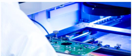
In order to maximize the use of circuit board space, I believe that many design partners will try to place components against the edge of the board, but in fact, this approach will bring great difficulties to production and PCBA assembly, and even lead to the inability to weld and assemble!
Layout hazards of board side devices
Forming plate edge milling plate
When components are placed too close to the edge of the board, the pads of the components will be milled off when forming and milling the board. Generally, the distance between the pads and the edge should be greater than 0.2 mm, otherwise the pads of the board side components will be milled off and the components cannot be welded after assembly.
Forming plate edge V-CUT
If the board edge is assembled with V-CUT, the components need to be further away from the board edge, because the V-CUT knife passes through the middle of the board, and the distance between the components and the board edge of the V-CUT should be more than 0.4mm. Otherwise, the V-CUT knife may damage the solder pad, causing the components to be unable to be welded.
Component interference equipment
When designing, the layout of components is too close to the edge of the board, which may interfere with the operation of automatic assembly equipment when assembling components, such as wave soldering or reflow soldering machines.
Equipment crashing components
The closer the components are to the board edge, the greater the potential interference they have on the assembly equipment. For components such as large electrolytic capacitors, which are relatively high, these components should be placed farther away from the edge of the circuit board than other components.
Damaged components on the sub board
After the product assembly is completed, the assembled product needs to be separated from the plate. During separation, components that are too close to the edge may be damaged, which may be intermittent and difficult to detect and debug.
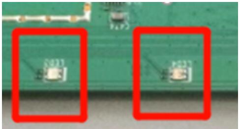
Let's share a production case about the insufficient distance between board edge components, resulting in damage~
Problem Description
During SMT placement of a product, it was found that the LED lamp was relatively close to the edge of the board, making it easy to be hit during production.
Problem Impact
During production and transportation, as well as when the DIP process crosses the track, LED lights may be damaged, affecting the function of the product. Problem Extension
It is necessary to modify the board, move the LED inside the board, and also involve changes to the structural light guide column, causing serious delays in the project development cycle.
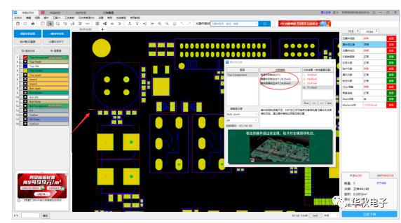
Board edge device risk detection
The importance of component layout design is self-evident, ranging from affecting welding to directly causing component damage. How can we ensure zero design issues and successfully complete production?
The DFM assembly analysis function has the ability to define inspection rules based on the parameters between component types and board edges. There are also specific inspection items for component layout at board edges. Multiple detailed inspection items such as high component to board edges, low component to board edges, and component to machine guide rail edges can fully meet design requirements for evaluating the safety distance between components and board edges.
After the PCB drawing design is completed, directly use Huaqiu DFM to conduct assembly inspection, which can avoid damage to components on the board side and affect the operation of production equipment during the assembly and production process. In short, the production problems encountered have been fully considered and avoided in advance to reduce costs and improve efficiency!
Its assembly analysis function has 10 major and 234 detailed inspection rules, covering all possible assembly issues, such as device analysis, pin analysis, pad analysis, and so on. It can solve various production situations that engineers cannot predict in advance.
Factory address: Mintai Industrial Park, Guantang Road, Huangjiang Town, Dongguan City, Guangdong Province
Office Address: Room 801, Dongtang Yongdongxing Building, Shajing Street, Bao'an District, Shenzhen
86-0755-33134847
86-0755-29868282


