

[Collection] Remember these PCB wiring points, you are the most beautiful child in the factory (3)
Article source:PCBworld Dated :2023/01-01
Conduct wiring according to the 50 ohm impedance line width, try to exit the wire from the center of the pad, make the wire straight, and try to walk on the surface layer. Make a 45 degree angle or circular arc routing at the place where you need to turn. It is recommended to turn on both sides of the capacitor or resistor. If you encounter device wiring matching requirements, please strictly follow the reference value length on the datasheet. For example, the requirements for the wiring length between an amplifier tube and a capacitor (or the wiring length between inductors), etc.
12. The role of network systems in cabling In many CAD systems, cabling is determined based on the network system. "Although the grid is too dense, the path size has increased, but the step size is too small, and the amount of data in the graph field is too large, which inevitably imposes higher requirements on the storage space of the device. At the same time, it also has a significant impact on the computing speed of computer-based electronic products.". "Some paths are invalid, such as those occupied by the pads of the component legs or by mounting holes or anchor holes.". Too sparse grids and too few paths have a significant impact on the distribution rate. Therefore, it is necessary to have a reasonably dense grid system to support the routing process. The distance between the legs of a standard component is 0.1 inch (2.54mm), so the foundation of a grid system is generally set to be 0.1 inch (2.54mm) or an integer multiple of less than 0.1 inch, such as 0.05 inch, 0.025 inch, 0.02 inch, etc.
13. Design Rule Check (DRC) After the completion of the wiring design, it is necessary to carefully check whether the wiring design conforms to the rules formulated by the designer, and also to confirm whether the rules formulated meet the requirements of the printed board production process. Generally, the inspection includes the following aspects: (1) Whether the distance between wires and wires, between wire and component pads, between wire and through-hole, between component pads and through-hole, and between through-hole and through-hole is reasonable, Whether the production requirements are met.
(2) Is the width of the power and ground wires appropriate, and is there tight coupling (low wave impedance) between the power and ground wires? Is there any place in the PCB where the ground wire can be widened.
(3) Whether the best measures have been taken for key signal lines, such as the shortest length, adding protective lines, and clearly separating the input and output lines.
(4) Whether the analog circuit and the digital circuit have separate ground wires.
(5) Whether the graphics (such as icons and labels) added to the PCB will cause a signal short circuit.
(6) Modify some undesirable alignments.
(7) Is there a process line added to the PCB? Whether the resistance welding meets the requirements of the production process, whether the resistance welding size is appropriate, and whether the character mark is pressed on the device pad to avoid affecting the electrical assembly quality.
(8) Whether the outer frame edge of the power supply layer in the multi-layer board is reduced, such as whether the copper foil of the power supply layer is exposed outside the board, which can easily cause a short circuit.
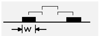
14. Check the 3W and 3H principles. In order to reduce crosstalk between lines, ensure that the line spacing is large enough. When the line center spacing is not less than 3 times the line width, 70% of the electric field can be maintained without mutual interference, which is called the 3W rule. To achieve 98% of the electric field without mutual interference, a spacing of 10W can be used.
(1) The routing of clock, reset, signals above 100M, and some key bus signals with other signal lines must meet the 3W principle. There is no longer parallel routing between the same layer and adjacent layers, and the number of vias on the link should be minimized. (2) There is a problem with the number of vias for high-speed signals. In some device guides, there are generally strict requirements for the number of vias for high-speed signals. In addition to the necessary pin fanout vias, it is strictly prohibited to drill extra vias in the inner layer. They have routed 8G PCIE 3.0 cables and also drilled 4 vias, which is no problem. (3) The center distance between clocks and high-speed signals on the same layer must strictly meet 3H (H is the distance from the routing layer to the reflux plane); Signals from adjacent layers are strictly prohibited from overlapping, and it is recommended to also meet the 3H principle. There are tools available to check for the above crosstalk issues.
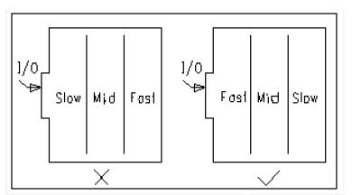
The main purpose is to prevent mutual interference between modules with different operating frequencies, while minimizing the wiring length of the high-frequency part.
For hybrid circuits, there are also ways to arrange analog and digital circuits on both sides of a printed circuit board, using different layers for wiring, and separating them with layers in the middle.
Factory address: Mintai Industrial Park, Guantang Road, Huangjiang Town, Dongguan City, Guangdong Province
Office Address: Room 801, Dongtang Yongdongxing Building, Shajing Street, Bao'an District, Shenzhen
86-0755-33134847
86-0755-29868282


